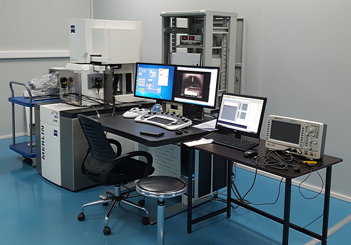
Recently, the Institute of Electrical Engineering, the National Institute of Metrology, and the National Center for Nanoscience and Technology, developed the first traceable metrology scanning electron microscope (M-SEM) system in China.
The laser interferometer, measuring optical mirrors and nanometer resolution displacement stage was assembled on the high resolution field emission scanning electron microscope. A novel scanning method based on stage moving step by step was established for replacing the ordinary SEM obtaining image operation. This new method can establish relationship between each SEM image pixel and the corresponding stage’s x/y coordinates which are obtained by laser interference method. The line width measuring value traceability of the nanometer sample structure was realized. The measuring errors produced by magnify fluctuation and scanning coils nonlinearity influence is minimized during the nano-scale dimension measuring. So the traceable metrology imaging process was accomplished for the sample with nanometer structure.
The M-SEM system is really important to enact nanometer dimension metrology standards, calibrate the SEM and other nanometer measuring equipment, calibrate the nano-scale standard reference materials, and join the international dimension measurement comparison.